Cyclone V GX Video Development System
Altera Cyclone V GX FPGA Development Board
Featured devices
- Cyclone V GX FPGA - 5CGXFC7D6F31C7NES
- MAX ®
V CPLD - 5M2210ZF256C4N (system controller)
- MAX
II CPLD - EPM240M100C4N (embedded USB-BlasterTM
II)
- MAX
II CPLD- EPM240M100C4N (optional, third party security CPLD feature)
Configuration
- Embedded USB-Blaster II (JTAG)
- Fast Passive Parallel (PFL)
- Push buttons, DIP switches and LEDs
Memory devices
- Two banks x40 bit DDR3 SDRAM with error correction code (ECC)
- 512Mb flash memory and 18MB SRAM
Standard communication ports
- USB 2.0
- Gigabit Ethernet
- PCIe x4 Edge Connector
- Universal high-speed mezzanine card (HSMC) (x 4 Xvcrs, x16 Tx LDVS, x16 Rx LVDS)
- One serial digital interface (SDI) channel
- Two SMAs for one transceiver channel
Clocking
- Programmable clock generator for FPGA reference clock input
- 125 MHz LVDS oscillator for FPGA reference clock input
- 148.5/148.35 MHz LVDS VCXO for FPGA reference clock input
- 50 MHz single-ended oscillator for FPGA and MAX
V FPGA clock input
- 100-MHz single-ended oscillator for MAX
V FPGA configuration clock input
- SMA input (LVPECL)
Power
- Laptop DC Input 14 – 20V adapter
- PCIe Edge Connector
System Monitoring Circuit
- Power (Voltage, Current, Wattage)
Mechanical
- PCIe card standard size (6.600" x 4.199")
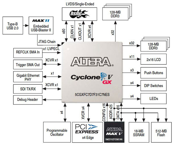
Altera Cyclone V GX FPGA Development Board Block Diagram

Terasic DVI-HSMC Card
Digital Transmitter
- One DVI transmitter with single transmitting port
- Digital Visual Interface (DVI) Compliant
- Supports resolutions from VGA to UXGA (25 MHz – 165 MHz Pixel Rates)
- Universal Graphics Controller Interface
- 12-Bit, Dual-Edge and 24-Bit, Single-Edge Input Modes
- Adjustable 1.1 V to 1.8 V and Standard 3.3 V CMOS Input Signal Levels
- Fully Differential and Single-Ended Input Clocking Modes
- Standard Intel 12-Bit Digital Video Port Compatible as on Intel™ 81x Chipsets
- Enhanced PLL Noise Immunity
- On-Chip Regulators and Bypass Capacitors for Reducing System Costs
- Enhanced Jitter Performance
- No HSYNC Jitter Anomaly
- Negligible Data-Dependent Jitter
- Programmable Using I²C Serial Interface
- Single 3.3-V Supply Operation
Digital Receiver
- One DVI receiver with single receiving port
- Supports UXGA Resolution (Output Pixel Rates Up to 165 MHz)
- Digital Visual Interface (DVI) Specification Compliant
- True-Color, 24 Bit/Pixel, 16.7M Colors at 1 or 2-Pixels Per Clock
- Laser Trimmed Internal termination Resistors for Optimum Fixed Impedance Matching
- 4x Over-Sampling
- Reduced Ground Bounce Using Time Staggered Pixel Outputs
- Lowest Noise and Best Power Dissipation Using TI PowerPAD™ Packaging

