FPGA
- Intel Stratix 10 GX/SX FPGA
FPGA Configuration
- On-Board USB Blaster II or JTAG header for FPGA programming
- Avalon-ST (AVST x8) configuration via MAX V CPLD and CFI flash memory
- ASx4 Configuration
Memory
- 128MB FLASH
- Up to 8 GB DDR4 2666/2400(FPGA Core Speed 1/2 FPGA) for each socket
Communication and Expansion
- Four QSFP28 connectors for 100/40/25/10 GbE network interface
- PCI Express Gen3 x16 edge connector (includes PCIe drivers)
- 2x5 Timing expansion header
Others
- General user input / output:
- 4 LEDs
- 2 push-buttons
- 2 slide switches
- U.FL clock input / output
- On-Board Clock
- 50MHz Oscillator
- Programmable Clock Generator
- System Monitor and Control
- Temperature sensor
- Power Monitor
- Fan control
- Power
- PCI Express 2x4 power connector for 12V DC Input
- PCI Express edge connector power
- Mechanical Specification
- PCI Express standard height and 3/4-length
Supported Memory Modules for Sockets
- DDR4-2666/2400 for FPGA Core Speed 1/2 FPGA
- QDRII+ 550MHz 144MBits
- QDRIV 1066MHz 144MBits
Block Diagram
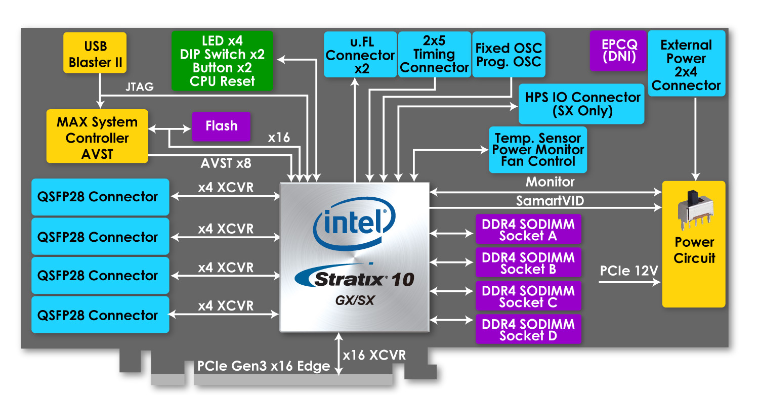
Note, DDR4A is shared with FPGA and HPS.
Memory Sockets
The four DDR4 SODIMM sockets are divided into two groups.
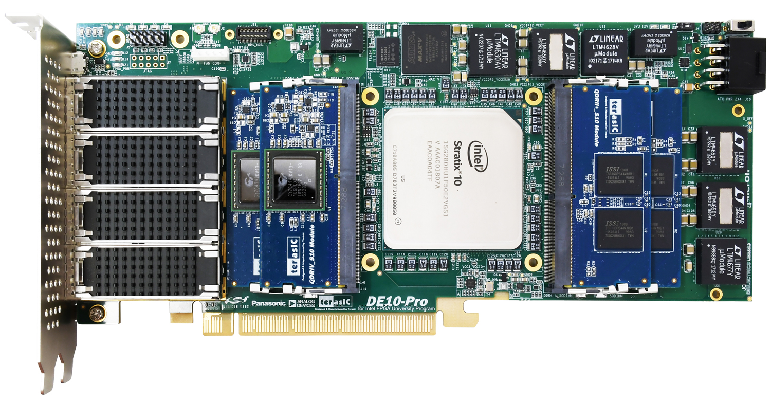
For better user flexibility, two different memory modules can be inserted separately in right & left groups. For example, users can insert two DDR4 modules on the right side and two QDRII+ SRAM modules on the left side.
Limitation: The two SODIMM sockets must be inserted with the same memory to prevent dysfunction on memory module that requires higher voltage.
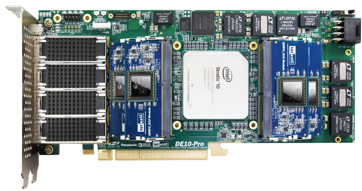
- Four QDR-IV Modules
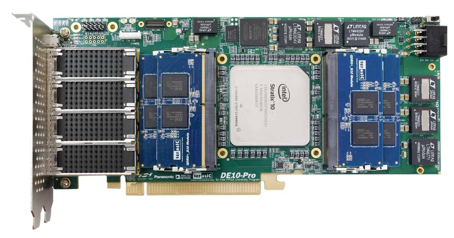
- Four QDR-II+ Modules
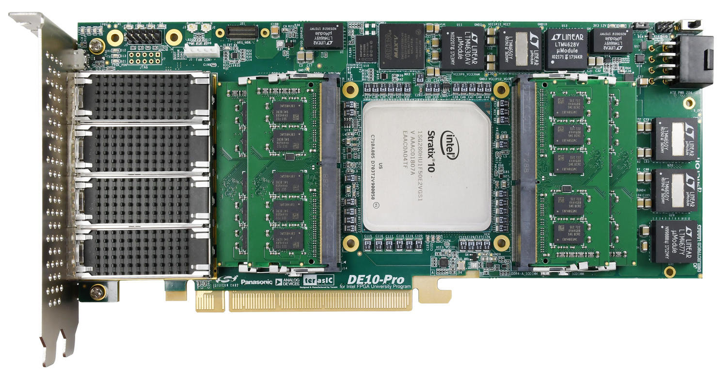
- Four DDR4 SODIMM Modules
- Two QDR-IV Modules, two QDR-II+ Modules
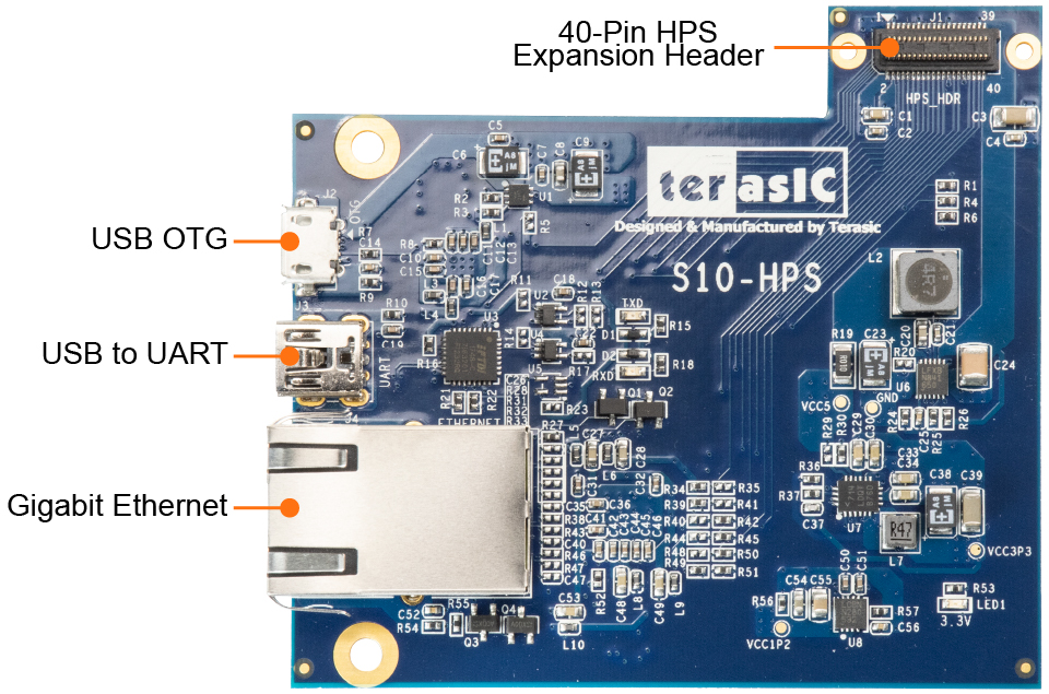
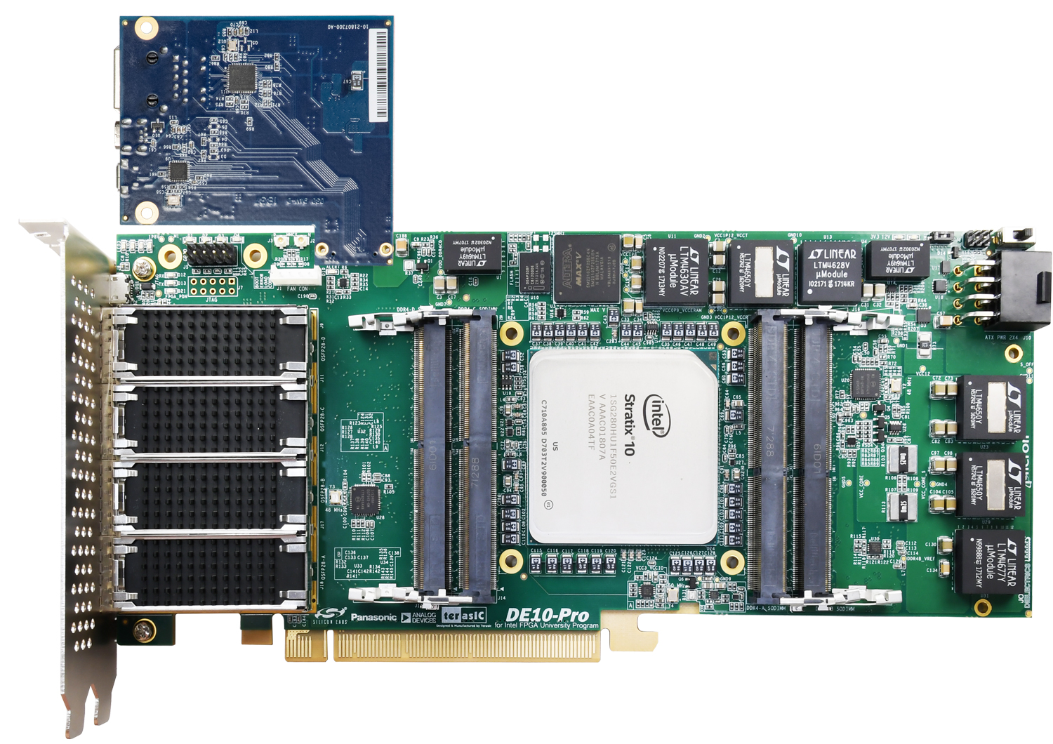
HPS Daughter Card
S10-HPS
