
如何选择适合的 FPGA 开发板?
请查看 FPGA 开发板指南页面,详列出不同型号之间的规格差异。
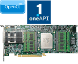
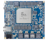
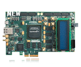
Agilex 7
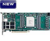
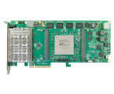
- Intel Agilex® 7 SoC FPGA I-Series AGIB027R29A1E2V
- Two QSFP-DD Ports and Two MCIO 8x Connectors
- Four Independent DDR4 SODIMM
- HPS System inclues pheriperal DDR4, SD card, UART, USB, Ethernet
- Supports PCIe, CXL
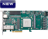
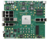
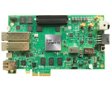
- Intel Agilex 7 SoC FPGA F-series AGFB027R24C2E2V
- QSFP28 port and FMC+ expansion connector
- Two independent DDR4 banks
- HPS system includes pheriperal DDR4, SD card, UART and Ethernet
- PCIe Gen4 x8
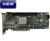
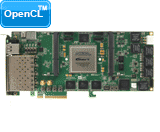
The Agilex™ 7 FPGA I-Series Transceiver SoC development kit delivers a complete design environment that includes both hardware and software for developing with Agilex™ 7 FPGA I-Series that contain 4x F-Tiles.
The Agilex™ 7 FPGA I-Series development kit delivers a complete prototyping and reference platform for designs needing PCI Express (PCIe) 5.0, Compute Express Link (CXL), or 400G Ethernet connectivity.
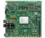
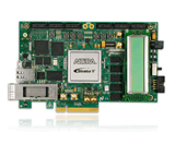
The Intel Agilex® 7 FPGA development kit provides a hardware development platform for evaluating the performance and features of the Intel Agilex® 7 FPGA F-Series with two F-tiles. It is a general purpose evaluation board in PCIe form factor with HPS hardware features.
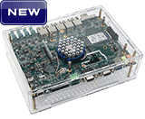
- Intel Agilex® SoC Standalone Module with onboard USB-Blaster II
- FMC+ and FMC connectors for expansion
- Support two independent 32GB DDR4 with ECC and one on-board QSFP28 connector
- Ideal for Prototyping, Industrial Control System
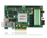
The Intel Agilex® 7 FPGA F-Series development kit delivers a complete design environment that includes all the hardware and software within a PCI Express (PCIe) form factor you need to start taking advantage of the performance and capabilities available in Intel Agilex® 7 FPGA F-Series FPGAs with P-Tile and E-Tile for your design needs.
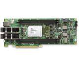
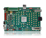
The Intel Agilex® 7 FPGA F-Series Transceiver-SoC development kit offers a complete design environment that includes hardware and software for developing Intel Agilex® 7 FPGA F-Series designs. This kit is recommended for developing custom Arm processor-based SoC designs and evaluating transceiver performance.
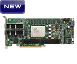
- Intel® Agilex™ F-Series FPGA AGFB014R24B2E2V
- Two QSFPDD connectors for 200/100/40/25/10 GbE network interface
- Four independent DDR4 SODIMM sockets
- PCIe Gen4 x16
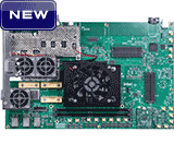
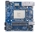
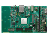
Agilex 5
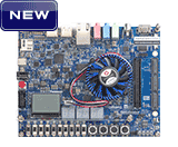
- Agilex 5 SoC with Quar-core ARM Cortext A55 and A76
- FPGA: SDRAM, DDR4, HDMI Out, MIPI, Video-In, ADC Header, GPIO/HSMC Headers
- HPS: DDR4, USB Host, MicroSD Socket, Ethernet, RTC, GPIO Header
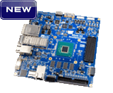
- Intel® Agilex® 5 E-Series with 656K LEs and HPS includes Dual Core A55 + Dual Core A76
- HPC FMC+, 2x20 GPIO and 2x6 TMD connector (one each for expansion)
- One 2.5 G Ethernet, HDMI output, two 2-lane MIPI, one QSFP+ and PCIe cabling Gen 3 x4 socket
Agilex 3
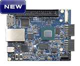
- Altera Agilex 3 FPGA with 135K Logic Elements
- 64MB 32-bit SDRAM and MicroSD Card
- HDMI Output (1080p Full HD)
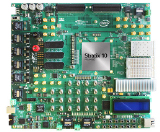
Stratix 10

- Stratix 10 1SX110HN3F43I2VG
- 32-pairs 12.5 Gbps Transceivers TX/RX
- 154 LVDS
- Dual 4GB 64-bit DDR4
- USB 3.1
- QSPI Flash and eMMC
- HPS Subsystem
- Power by 12V
- 98 mm x 86mm
- Interface: FMC+ Connector x2
- Intel Stratix 10 SoC Standalone Module with onboard USB-Blaster II
- FMC+ and FMC connectors for expansion
- Support two independent 32GB DDR4 with ECC.
- Ideal for Prototyping, Industrial Control System, Military and Aerospace
- Intel® Stratix® 10 MX FPGA H-Tile(8 GB/16 GB)
- On-board 8GB DDR4 , one DDR4 DIMM and one HiLo connector supporting DDR4 and QDR-IV
- Two QSFP28 optical interface port
- PCIe Root and End Point connector
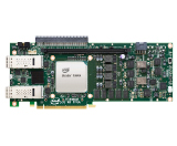
- Intel® Stratix® 10 TX 280 F2912 FPGA
- One FMC+ connector
- Two QSFPDD 1x1, one QSFPDD 2x1 and two QSFPDD 1x2 optical transceiver interface
- 1SX280HU2F50 Intel® Stratix® 10 SoC FPGA
- One HiLo DDR4 memory card (4GB)
- One DDR4 SODIMM memory card (16GB dual rank)
- Two HPS peripheral daughter cards (OOBE and NAND)
- Two FMC loopback cards supporting transceiver, LVDS and single-ended I/Os
- Two quad small-form-factor pluggable (QSFP28) and one SFP+ port
- Two FMC+ low-pin count (LPC + 15 transceivers) connector
- One SFP+ interface
- PCIe x16 edge connector (via cable - not included)
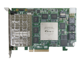
- Intel® Stratix® 10 DX FPGA
- On-board DDR4 SDRAM (8GB) and 2 DDR4 DIMM (8GB each)
- Two quad small-form-factor pluggable (QSFP56) cages
- PCIe Gen4x16 Endpoint via Edge Connector
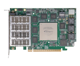
- Intel Stratix 10 GX/SX FPGA
- Four QSFP28(100GbE) connectors and one PCI Express (PCIe) x16 edge connector
- Four independent DDR4 SODIMM sockets (work with DDR4/QDR-II+/QDR-IV)
- Evaluate transceiver channel performance
- Generate and verify pseudo-random binary sequence (PRBS) patterns via an easy-to-use GUI
- Dynamically change the channel's differential output voltage (VoD), pre-emphasis, and equalization settings to optimize the performance for your channel
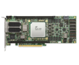
Stratix V
- Stratix V GX 5SGXEA7N2F45C2N
- DDR3 SO-DIMM and FMC x4 Connectors
- Large ASIC Prototyping Applications
- Altera Stratix® V GX FPGA (5SGXEA7N2F45C2)
- 32MB SRAM (ISSI QUADP for DE5-Net 450, GSI SigmaQuad-II+ for DE5-Net 550, Cypress QDRII+ for DE5-Net 500)
- Up to 8GB DDR3 800 MHz SO-DIMM SDRAM
- Stratix V GX FPGA 5SGXEA7K2F40C2N
- DDR3 SDRAM, QDR II+ SRAM, RLDRAM II
- PCIe x8, HSMC, SDI, QSFP, Gigabit Ethernet
- Stratix V GS FPGA: 5SGSMD5K2F40C2N
- DDR3 SDRAM, QDR II+ SRAM, RLDRAM II
- PCIe x8, QSFP, Gigabit Ethernet, SDI, HSMC
- Stratix V GX FPGA 5SGXEA7N2F40C2N
- Configuration flash
- 28 full-duplex transceiver channels
- Featured device: 5SGXEA7N2F45C2N
- DDR3 SDRAM, QDR II
- QSFP, SFP+, SMA, CFP, Interlaken interface, Gigabit Ethernet
Stratix IV
- Stratix IV GX EP4SGX230/EP4SGX530 带高速收发器
- 2 个PCIe x4 连接器和一个 DDR3 SO-DIMM 槽
- 可实现多 FPGA 系统的堆叠设计
Arria 10
- Intel® Arria® 10 GX FPGA with 1150K logic elements
- Total 8 GB DDR4-2133 memory
- 1024Mb QSPI Flash
- One Thunderbolt™ 3 port for host communication and on-board USB-Blaster II function
- Power/temperature monitor and auto fan speed control
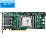
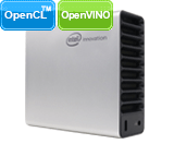
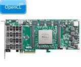
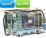
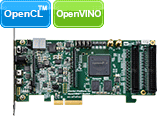
- Intel Arria 10 GX FPGA (10AX115N2F45E1SG)
- Low Profile PCIe Gen3 x16 (Dual PCIe Gen3 x8) Board
- Two QSFP+ Connectors
- Five Independent 550MHz QDRII+ SRAMs
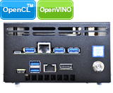
- Build-in OpenVINO Toolkit
- Intel Arria 10 GX FPGA (10AX115S2F45I1SG)
- Intel Core™ i5/i7 Processor
- Arria 10 SoC with Dual-core ARM Cortex-A9
- DDR4, HDMI, FMC, PCIe, SATA, Ethernet, Flash, USB, etc.
- Type-C USB 3.1 Gen1 and DisplayPort Altenate Mode
- Support Linux BSP
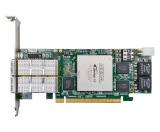
- Intel Arria 10 GX 10AX115S2F45I1SG FPGA
- Six full-duplex transceiver channels with 2.4 mm SMA connectors
- Transceiver channels to Amphenol Xcede+ backplane connector, QSFP+,CFP2 and SFP+ optical interface
- Arria 10 GX FPGA (10AX115S2F45I1SG)
- 1 GB DDR4 SDRAM, 2GB DDR3 SDRAM, and RLDRAM3 (16 Meg x 36) daughtercards
- One QSFP and one SFP+ connectors, one PCI Express (PCIe) x8 edge connector
- Two FMC low-pin count (LPC + 15 transceivers) connector
- Arria 10 GX FPGA (10AX115N2F45E1SG)
- Half-length PCIe Gen3 x8 board
- Four QSFP+ connectors
- Six independent 550MHz QDRII+ SRAMs
- Arria 10 GX FPGA (10AX115N2F45E1SG)
- Half-length PCIe Gen3 x8 board
- Four QSFP+ connectors
- Six independent 550MHz QDRII+ SRAMs
- Altera Arria 10 GX FPGA (10AX115N2F45E1SG)
- Four QSFP+ connectors and one PCI Express (PCIe) x8 edge connector
- Two independent DDR4 SODIMM socket and four independent 550MHz QDRII+ SRAMs
- Evaluate Intel® Arria® 10 SoC device features and performance.
- Begin development of your hardware and software design.
- Use as a platform for target reference designs, OS/BSP, and tools.
- Altera Arria 10 GX FPGA (10AX115N2F45E1SG)
- 4 QSFP+ 连接器和 PCI Express (PCIe) x8 边缘连接器 (提供 Windows PCIe 驱动)
- 2 个独立 DDR3 SODIMM 插槽和 4 颗独立 550MHz QDRII+ SRAM
Cyclone 10
- Intel® Cyclone® 10 LP FPGA (10CL025, U256 package)
- 128Mb HyperRAM and 64Mb EPCQ Flash
- Gigabit Ethernet port, 2x20 GPIO Expansion Header , Pmod compatible connector and Arduino UNO R3 type connectors
Cyclone V
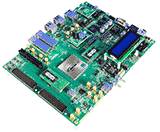
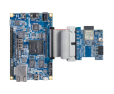
PIB是一个基于Intel x86 和FPGA的开发平台,针对工业的边缘计算,和控制,以及更多。利用了FPGA的芯片可编程,和CPU的软件可编程能力,共同创造了一个巨大的创意空间。在这里,你可以同时得到i7 core CPU的算力,和FPGA对于接口的并行处理能力,短延时,确定性计算的创造力。
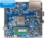
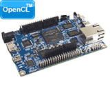
- Cyclone V SoC with Dual-core ARM Cortex-A9 (HPS)
- Wi-Fi, using ESP-WROOM-02 module
- Bluetooth SPP, using HC-05 module, up to 10 meter range
- Arduino Expansion Header (Uno R3 Compatibility), Full HD HDMI Output, UART-to-USB, USB OTG Port, Micro SD Card Socket, Gigabit Ethernet and GPIO Headers
- Cyclone V SoC with Dual-core ARM Cortex-A9 (HPS)
- Wi-Fi, using ESP-WROOM-02 module
- Bluetooth SPP, using HC-05 module, up to 10 meter range
- Arduino Expansion Header (Uno R3 Compatibility), Full HD HDMI Output, UART-to-USB, USB OTG Port, Micro SD Card Socket, Gigabit Ethernet and GPIO Headers
- Bundled with Terasic Starter Platform for OpenVINO™ Toolkit and Intel IoT Dev. Kit (UP2)
- Use FPGA as OpenVINO hardware acceleration engine and provide pre-compiled FPGA bitstream
- Ideal coding environment for OpenVINO developer as standalone system
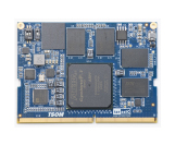
- SoC System on Module
- Cyclone V SoC with Dual-core ARM Cortex-A9 (HPS)
- Cyclone V GT PCIe Board, 301K LE, PCIe
- 1GB DDR3, 64MB SDRAM, EPCQ256
- UART-to-USB, GPIO and Arduino Headers
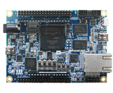
- Cyclone V SoC with Dual-core ARM Cortex-A9 (HPS)
- On-board two high speed A/D conveters
- 1GB DDR3 SDRAM (32-bit data bus)(HPS)
- Arduino Expansion Header (Uno R3 Compatibility), UART-to-USB, USB OTG Port, Micro SD Card Socket, Gigabit Ethernet and GPIO Headers
- DE0-Nano-SoC 主板为基础下, 把DCC (AD/DA Data Conversion Card) 子卡上的高速ADC 电路内建于主卡上. 非常适合于需要高速ADC 应用的系统.
- 内建的ADC 电路以SMA 做为输入介面, 提供两个通道, 每个通道有14-bit 解析度, sample rate 可高达 150MSPS(Mega-Samples Per Second).
- Cyclone V SoC with Dual-core ARM Cortex-A9 (HPS)
- 1GB DDR3 and 64MB SDRAM
- VGA Out, Video-In, UART-to-USB, USB Host x2, Micro SD Card Socket, 1Gbps Ethernet, and HSMC/GPIO Headers
- 800x480 5-point touch, 8Mega Pixel Camera, 9-axis sensor and amblient light sensror
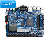
- Intel Cyclone V SoC FPGA,ARM Cortex-A9 双核 HPS
- FPGA:SDRAM,VGA 输出,Video 输入,ADC 接头,GPIO 接头,HSMC 接头
- HPS:DDR3,USB Host 端口,MicroSD 卡槽,以太网,UART 转 USB,LTC 接头
- 支持 Linux BSP 和 openCL BSP
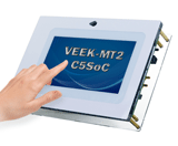
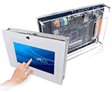
- Cyclone V SX SoC—5CSXFC6D6F31C6N (SoC)
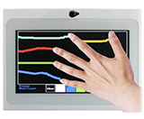
- 8-Megapixel Digital Image Sensor Module with auto focus
- 7" LCD Touch Screen Module with 5 point touch
- Accelerometer, Gyroscope, Magnetometer, Ambient Sensor
- Cyclone V SoC with Dual-core ARM Cortex-A9 (HPS)
- 1GB DDR3 SDRAM (32-bit data bus)(HPS)
- Arduino Expansion Header (Uno R3 Compatibility), Full HD HDMI Output, UART-to-USB, USB OTG Port, Micro SD Card Socket, Gigabit Ethernet and GPIO Headers
- Cyclone V SoC with Dual-core ARM Cortex-A9 (HPS)
- 1GB DDR3 SDRAM (32-bit data bus)(HPS)
- Arduino Expansion Header (Uno R3 Compatibility), UART-to-USB, USB OTG Port, Micro SD Card Socket, Gigabit Ethernet and GPIO Headers
- Cyclone V 5CEBA4F23C7N Device
- 4-bit Resistor VGA
- Provides SPI and 4-bit SD mode for SD Card access
- Serial Configuration device – EPCS64
- 64MB SDRAM, x16 bits data bus
- On-Board USB Blaster (Normal type B USB)
- Cyclone V SoC with Dual-core ARM Cortex-A9 (HPS)
- 1GB DDR3 and 64MB SDRAM
- VGA Out, Video-In, UART-to-USB, USB Host x2, Micro SD Card Socket, 1Gbps Ethernet, and GPIO Headers
- Touch & LCD Spec
- Cyclone V SoC with Dual-core ARM Cortex-A9 (HPS)
- 1GB DDR3 and 64MB SDRAM
- VGA Out, Video-In, UART-to-USB, USB Host x2, Micro SD Card Socket, 1Gbps Ethernet, and GPIO Headers
- Cyclone V GX 5CGXFC5C6F27C7N Device
- LPDDR2, SRAM, FLASH EPCQ256
- Arduino Header, 2x20 GPIO Header, HSMC, UART to USB, HSMC, HDMI TX
- Cyclone V SX SoC—5CSXFC6D6F31C6N (SoC)
- Hard processor system (HPS)
- DDR3, QSPI Flash, Micro-SD Card
- FPGA prototyping
- FPGA power measurement
- Transceiver I/O performance up to 5.0 Gbps
- PCI Express® (PCIe® ) Gen2 x4 (at 5.0 Gbps per lane)
- Endpoint or rootport support
Cyclone IV
- Cyclone IV EP4CE115 with ~114,480 LEs
- 8-Megapixel Digital Image Sensor Module
- 7" LCD Touch Screen Module
- Ideal for use with embedded soft processors
- Tiny and robust packaging for portable applications
- Expansion headers for daughter cards, motors, actuators, etc.
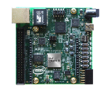
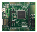
MAX 10
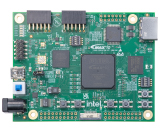
The Intel® MAX® 10 FPGA 10M50 Evaluation Kit provides an easy-to-use platform for evaluating the Intel® MAX® 10 FPGA technology and Intel® Enpirion® regulators.
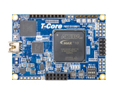
- MAX 10 10M50DAF484C7G Device
- QSPI Flash, Color LED, ADC and GPIO Header
- Support RISC-V
- USB-Blaster II for programming FPGA
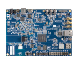
- MAX 10 10M50DAF484C6G with 50K LEs
- DDR3 with ECC, QSPI Flash, MicroSD Socket
- Ethernet, Audio codec, HDMI RX, Acceleromter, ADC, DAC

- MAX 10 10M50DAF484C7G Device
- Accelerometer and 4-bit Resistor VGA
- 64MB SDRAM, x16 bits data bus
- Arduino UNO R3 and 2x20 GPIO connector
- On-Board USB Blaster (Normal type B USB)
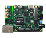
- Develop designs for the 10M50D, F484 package FPGA
- Measure the performance of the MAX 10 FPGA analog-to-digital block conversion
- Interface MAX 10 FPGAs to DDR3 memory at 300 MHz performance
- Run embedded Linux using the Nios® II processor
Intel® MAX® 10 FPGA Evaluation Kit is an entry-level board for the evaluation of the Intel® MAX® 10 FPGA technology.
- MAX 10 10M50DAF484C6G with 50K LEs
- DDR3 with ECC, QSPI Flash, MicroSD Card
- Ethernet, Audio codec, HDMI RX, Acceleromter, ADC, DAC
- 8-Mega pixel color camera and 7" 5-point touch screen