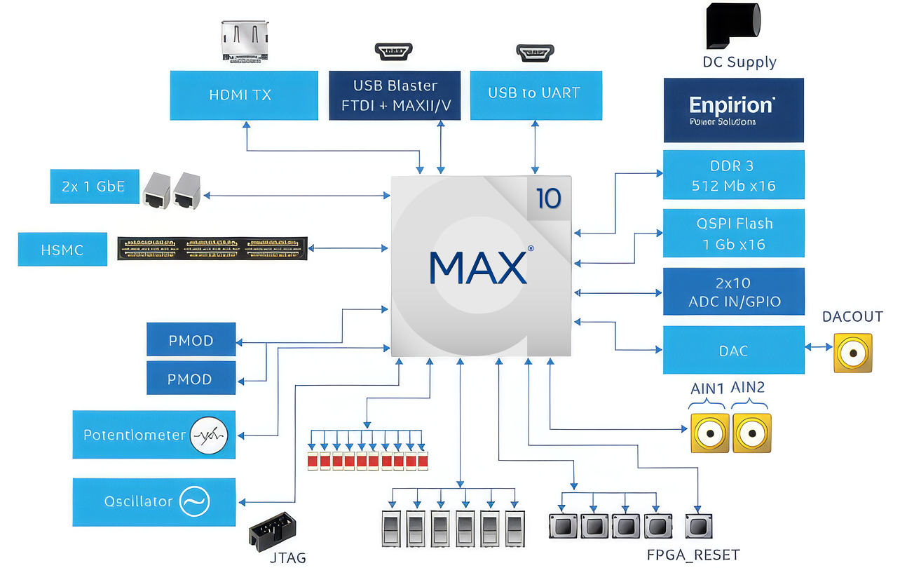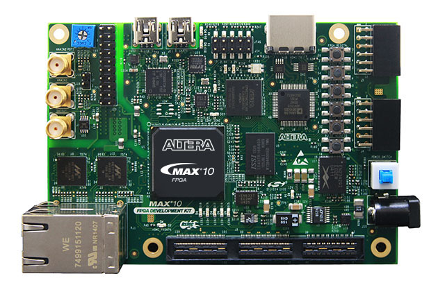
The MAX® 10 FPGA Development Kit provides a full featured design platform built around a 50 K logic elements (LEs) MAX® 10 FPGA, optimized for system level integration with on-die analog-to-digital converter (ADC), dual-configuration flash, and DDR3 memory interface support.
With this development board, you can:
- Develop designs for the 10M50D, F484 package FPGA.
- Measure the performance of the MAX® 10 FPGA analog-to-digital block conversion.
- Interface MAX® 10 FPGAs to DDR3 memory at 300 MHz performance.
- Run embedded Linux using the Nios® II processor.
- Interface to daughtercards and peripherals using HSMC and Digilent Pmod compatible connectors.
- Measure FPGA power (VCC_CORE and VCC_IO) using the power monitor graphical user interface (GUI).
- Reuse the kit’s PCB board and schematic as a model for your design.
MAX® 10 FPGA Development Board Block Diagram